How to Design a Low-Noise Amplifier for Audio Applications
Designing a low-noise amplifier for audio applications requires a careful balance of theoretical knowledge, component selection, and practical layout techniques. The goal is to preserve the integrity of the audio signal while minimizing any added noise that could degrade sound quality. Operational amplifiers serve as the core building block in many such designs, offering flexibility in gain configuration and frequency response. This article outlines a structured approach to designing a low-noise amplifier using operational amplifiers, focusing on the key areas that influence noise performance.
The process begins with understanding the sources of noise within an amplifier circuit and then selecting components that minimize their contribution. Gain stage design, power supply decoupling, and printed circuit board (PCB) layout all play significant roles in achieving a low-noise result. By following a systematic methodology, designers can create audio amplifiers that maintain signal clarity without introducing unnecessary artifacts. The following sections explore each of these aspects in detail.
Circuit Pulse offers resources and tools that support engineers in this design process, though the principles discussed here apply broadly across different operational amplifier families. The emphasis is on methodology and context rather than specific product recommendations, allowing readers to adapt the information to their own requirements.
Understanding Noise Sources in Audio Amplifiers
Noise in an audio amplifier originates from multiple sources, each contributing to the overall noise floor. The operational amplifier itself generates both voltage noise and current noise, specified in the datasheet as nano volts per root hertz and pico amps per root hertz respectively. Resistors in the feedback network and any external biasing components introduce thermal noise, which is proportional to resistance value. Additionally, power supply ripple and electromagnetic interference can couple into the signal path if not properly mitigated.
The total noise seen at the output depends on the gain configuration and the impedance levels in the circuit. Lower impedance paths tend to reduce the impact of voltage noise from the op-amp, while higher impedance paths increase the effect of current noise. For audio applications, frequencies range from 20 Hz to 20 kHz, so the noise spectral density must be integrated over this bandwidth. Understanding these contributions allows the designer to make informed trade-offs between noise, bandwidth, and power consumption.
A common method for evaluating noise performance is to calculate the root-sum-square of all independent noise sources and then multiply by the circuit gain. This calculation provides an estimate of the output noise voltage, which can be compared to the desired signal-to-noise ratio. Designers often consider the noise figure as a figure of merit, though for audio applications the absolute noise floor matters more in terms of audibility.
Selecting the Right Operational Amplifier
Choosing an operational amplifier for a low-noise audio application involves reviewing key parametric specifications. Voltage noise density, current noise density, and total harmonic distortion plus noise (THD+N) are primary considerations. Many modern op-amps are designed specifically for audio and exhibit voltage noise below 1 nV/√Hz and extremely low distortion. However, the choice also depends on the required gain bandwidth, slew rate, and output drive capability.
For low-impedance sources such as moving coil microphones or high-quality line outputs, voltage noise tends to dominate. In these cases, an op-amp with the lowest possible voltage noise is desirable. For high-impedance sources like piezo pickups or certain sensors, current noise becomes more significant, and a FET-input op-amp with low current noise may be preferable. The trade-off between bipolar and FET input stages should be evaluated based on source impedance and the surrounding resistor values.
Designers must also consider the op-amp’s ability to drive capacitive loads, as audio cables and subsequent stages can present capacitive loading that leads to instability. Some audio op-amps include internal compensation or require external compensation networks. Reading the datasheet carefully and performing stability analysis using loop gain simulations helps ensure reliable operation. Circuit Pulse provides comparison tools that can assist in narrowing down suitable candidates for a given design target.
Gain Stage Design and Component Values
The feedback network around the operational amplifier sets the gain and also influences noise performance. Resistor values should be chosen to keep thermal noise low while maintaining acceptable DC accuracy and bandwidth. In a non-inverting configuration, the gain is set by the ratio of the feedback resistor to the ground resistor. Using lower resistance values reduces thermal noise but increases power dissipation and may load the op-amp’s output.
A practical approach is to select feedback resistors in the range of a few kilo-ohms. For example, a 10 kΩ feedback resistor with a 1 kΩ ground resistor provides a gain of 11 (about 20.8 dB). The thermal noise contributed by these resistors can be calculated using the Johnson-Nyquist formula. To minimize noise, some designers use metal film resistors with low tolerance and low noise coefficient. Additionally, the input resistor in the signal path should be kept as low as possible to reduce both thermal noise and the contribution from the op-amp’s current noise.
Capacitors in the signal path, such as DC-blocking capacitors, must be selected for low leakage and low dielectric absorption. Electrolytic capacitors are often avoided in critical audio paths unless bypassed with film capacitors. The feedback loop may include a small capacitor for stability, but its value should be chosen carefully to avoid excessive high-frequency roll-off or added phase shift. Simulation tools can help model the impact of component tolerances on overall noise and frequency response.
Power Supply Considerations for Low Noise
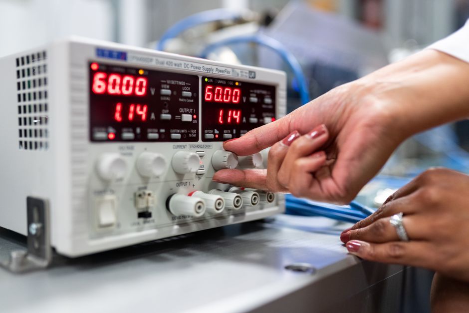
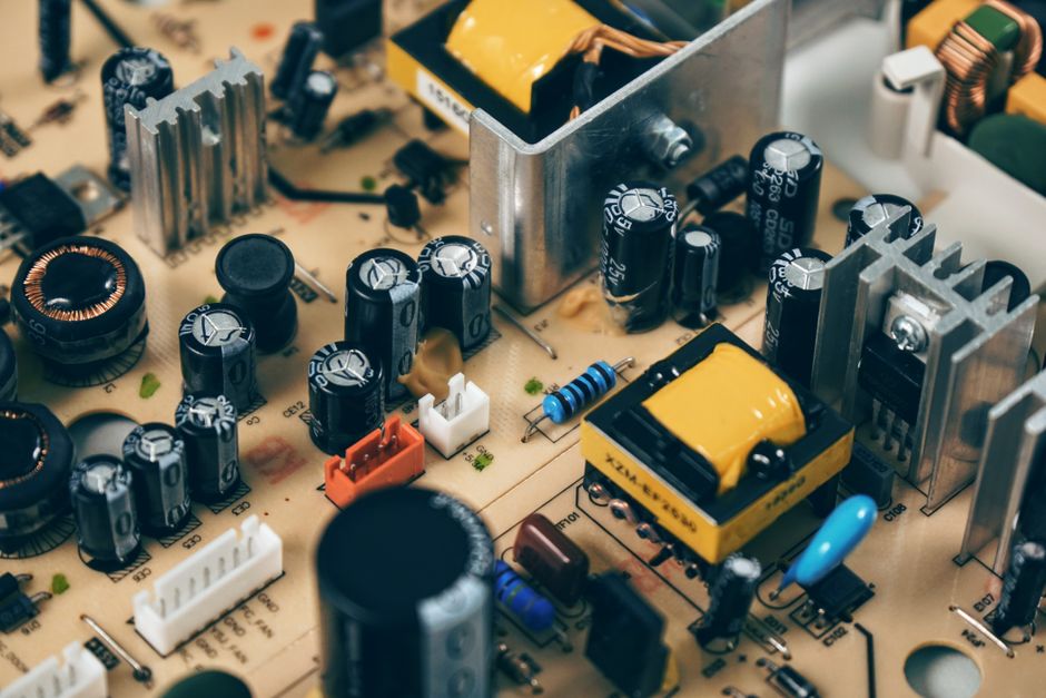
The power supply rail has a direct effect on amplifier noise. Any ripple or hum present on the supply will couple into the signal path through the op-amp’s power supply rejection ratio (PSRR). While modern op-amps have good PSRR at low frequencies, performance degrades at higher frequencies. Therefore, local decoupling is essential. A combination of bulk electrolytic capacitors and low-inductance ceramic capacitors placed close to the op-amp’s power pins helps filter out high-frequency noise.
Using separate analog and digital power supplies, or at least separate traces and ground returns, prevents digital switching noise from contaminating the audio circuitry. For battery-operated designs, a low-noise voltage regulator can be employed to provide a clean supply. The regulator’s output noise and transient response should be evaluated in the context of the amplifier’s requirements.
Grounding topology also matters. A star ground or a dedicated ground plane for analog signals helps minimize ground loops. The power supply return path should be kept separate from the signal ground until they meet at a single point. This practice reduces the potential for common-mode noise injection. Designers often consider using ferrite beads or Pi-filters on power lines for additional noise attenuation, though these components must be chosen to avoid resonances within the audio band.
PCB Layout Techniques for Reducing Noise
PCB layout is one of the most critical aspects of low-noise amplifier design. A solid ground plane is recommended for the audio section, as it provides a low-impedance return path and shields sensitive traces. However, care must be taken to avoid cutting the ground plane with long signal traces that create loops. Signal routing should be as short and direct as possible, especially for high-impedance nodes like the op-amp’s non-inverting input.
Analog and digital sections should be physically separated on the board. If both appear on the same PCB, a split ground plane with a single connection point (often under the ADC or DAC) can prevent digital return currents from flowing through analog ground. Additionally, analog signal traces should be kept away from high-speed digital lines and power switching circuits.
Bypass capacitors must be placed with very short traces to the op-amp pins. A typical arrangement uses a 10 µF electrolytic and a 0.1 µF ceramic in parallel, with the ceramic closest to the pin. Vias should be used to connect these capacitors directly to the ground plane. To further reduce noise, inputs and outputs can be shielded with guard traces or ground-filled areas. The overall layout should be reviewed for parasitic capacitance and inductance that could affect stability and noise bandwidth.